


Overview:
With the trend of lighter, thinner and
smaller product development, FPC is becoming a well-developed alternative of
the PCB in some product applications.
Ideal Jacobs is specialized in design support, quality and most importantly the cost control through years of support to elite customers. We further insert FPC into the membrane switches to help our customers enhance human-machine interfaces, to simply assembly with counterparts and to further improve the whole space of products especially for main PCB.
Flexible Printed Circuit largely improves the user experience and helps customer with more possibilities in product design by its compact size and light weight. It stretches freely in a three-dimensional space. Rigid-Flex PCB, on the other hand, can be an excellent support body of electronic components while being flexible.
Types of FPC:
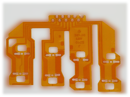

.jpg)
.jpg)
.jpg)
.jpg)

1) Single Layer of FPC
It has a layer of chemically etched conductive pattern, and
the conductive pattern layer on the surface of the flexible insulating substrate
is a rolled copper foil.
2) Double-sided FPC
The double-sided FPC has a conductive pattern made by
etching on both sides of the insulating base film, which increases the wiring
density per unit area.
3) Multilayer FPC
Multi-layer FPC is to laminate 3 or more layers of single-sided
or double-sided flexible circuits together, and form metallized holes by
drilling and electroplating to form conductive paths between different layers.
4) Rigid-Flex PCB
it includes two or more conductive layers that comprise either
flexible or rigid insulation material between each one. Both rigid and flexible
areas that make them ideally suited for a wide range of applications.
Basic Specification:
No. | Item | Producing Capability |
1 | Layers | 1-6 |
2 | Panel Size | Max:500X550mm |
3 | Drilling Diameter | Min. Diameter: 0.15mm(6mil) |
4 | Base Material Copper Thickness | Min:1/3 Oz |
5 | Insulating Layer Thickness | Min:0.0125mm(PI)(0.5mIL) |
6 | Electroplating Au Thickness | ≥0.05um |
7 | Chemical Immersion Ni/Au Thickness | 0.05um---0.1um |
8 | Etching Line Width & Space | S/S:2mil(0.05mm) |
9 | Etching Tolerance | Width:±10% |
10 | Outline Tolerance(from side to side) | ±0.05mm(:±2mil) |
11 | Parts Fixed Position Tolerance | ±0. 2mm(8mil) |
Office Hours
Monday through Friday 8:30am - 5:00pm
Phone: +0086-0592-5064000
Fax:+0086-0592-5074000
Email: inquiry.list@idealjacobs.com.cn
Request a free quote today for your next custom front panel, nameplate, membrane, or other overlay need. We will return your inquiry promptly.
Send your artwork and mechanical drawings to us via email using the link above. Our office will contact you when they have been received. Let us know if you have any questions.

Copyright © Ideal Jacobs (Xiamen) Corporation All Rights Reserved
If there is any infringement on the quoted font, text, and images, please contact us for deletion